Telling it like it is on the inside of production semiconductors as seen at Chipworks


Wednesday, August 26, 2015

Apple Watch and ASE Start New Era in SiP

Back in April the Apple watch appeared in our labs, and of course we analyzed it to see its contents. That set us some challenges, since inside the case we have the S1”chip” (as Jony Ive called it in the launch last year). As you can see, it occupies most of the space inside the case, so it’s a pretty large chip; normally only the likes of IBM or Nvidia make chips this large.


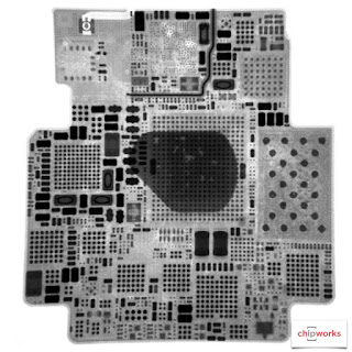
Actually, we knew that there had to be multiple chips inside the S1, because we did a pseudo-teardown last year, based on Apple’s promo video at the time. It turns out that the S1 is actually an assembly of chips on a dedicated printed circuit board (PCB) substrate, with over 30 chips plus many passive components. So it is more accurately described as a System-in Package (SiP).
This was confirmed when we took the S1 out of the case and x-rayed it;


And we identified many of them;


This gave us the teardown information that we needed to find what chips were used, but the S1 is so different from any of the other wearables that we have looked at, that we had to go in and see how it was put together. So cut it in two and then onto the polishing wheel, and we get an idea of what Apple’s assembly house has done for them.

Actually, we did two cross-sections along the lines shown here;


This is section P1AS2;


On the left is the Dialog PMU; in the centre is the Apple APU (APL0778), with an Elpida DRAM co-packaged; and at the right is the Sandisk 64-Gb flash, including the controller chip and a spacer die. There seemed to be a wide-spread assumption that the APL0778 would be in a Package-on-Package (PoP) stack with the memory, as in the iPhones, but here it is in a straight-forward two-die stacked package.

If we look closer, we can see that the S1 uses conventional assembly techniques, but once all the components are on the 4-layer PCB, the whole thing has been over-molded with more molding compound, and then plated with metal to give the stainless-steel looking finish. A close-up of the right edge shows what I mean;


There are two 32-Gb flash dies in a conventional package with its own substrate, which is flip-bonded onto the PCB, covered with the SiP over-molding, and the exterior is metallized, giving the silver finish.

Section P1AS1 has the Broadcom BCM4334 in the centre, and the AMS NFC booster chip on the right. At left is a co-axial RF test socket.


Again, if we look closely, we can see that underfill has been used across the whole PCB before the over-molding was performed. Another feature of note is the I-shaped EMI shielding on the right of the BCM die, molded into the SiP – this is the first time we have seen this in any sort of package. In the x-ray image above, it surrounds the BCM chip, separating it from the other components. Here we are in close-up;


In effect the complete S1 assembly has EMI shielding since (with the exception of the accelerometer/gyro) the whole thing has a metal coat, mostly copper with a skin of iron/chromium. Such a coating will also inhibit moisture ingress, a good thing since I’ve heard tales of folks showering while wearing a Watch, and wrists can get a bit sweaty anyway.

A big question for us is – who supplied such an innovative package? Press commentary has identified the provider as ASE (Advanced Semiconductor Engineering Inc.) of Taiwan; and I presented at an IMAPS wearables workshop back in June, and when I got to the Watch analysis the attendees from ASE shared a few knowing looks.

The last quarterly analyst call from ASE also included this graphic, which details quite nicely the SiP concept, and includes details such as the EMI shielding:


ASE has also had more revenue from SiP this quarter, “In terms of overall, the SiP revenue accounted for about 22% in the second quarter, up from 15 a quarter ago because of the EMS SiP product ramp up.” Interestingly, they are also running below break-even on the SiP product (In response to a question as to whether all SiP projects are losing money, or just the one; “Thank God it is. It's only this particular project that is running below break-even. Other things are moving very nicely.”).

Given these comments, I’m inclined to believe the press on this one – ASE is the supplier.

Another nugget comes from perusing the transcript of the call – “What kind of application and what kind of customers you are working with for the new SiP projects?

Tien Wu replied, “I don't think I'd comment specifically but I’m pretty sure you will find some new products that have come out pretty soon. Sorry.”

He also noted, “We promise each other will never come out specific customers. So I will give you a non-qualifying, non-specific answer. We are expanding the SiP coverage to the cellphone, to the tablet in that particular arena. Hopefully, we can report more revenue, more penetration.”

I take that to mean that we may well see this style of SiP in the new iPhone and iPad later this year – more fun!

Friday, April 10, 2015

Apple Watch Launch Confirms WiFi and NFC Inside


Today (April 10) is the day that the Apple Watch becomes available for order, and of course we will be buying some to see what’s inside. We won’t be going for the gold Edition model, even so some of us here would like to; the Sport version should be quite good enough.
At the Apple event back on March 9 it was almost a case of last and least for the Apple Watch, after listening through the ResearchKit and new MacBook launches, and more Apple Pay demos. The Watch presentation was almost a case of déjà vu, since we got most of the details last year in the announcement last September.
The one new technical detail that I did pick up on was that the use of WiFi was confirmed – there was no mention of that last year (time 74.00 in the March 9 video). There was also much emphasis on the ability to use Apple Pay and make calls through the Watch, so we know that there are microphones in there, and it has NFC (near-field communications) capability, but we knew that after the initial launch last year.
The WiFi news was interesting to us, since we did a pseudo-teardown back then, based on Apple’s promo video, and we came to the conclusion that the Broadcom BCM4334 was in the Watch. But no mention of WiFi – what gives? I guess they just forgot, and even in the new launch it was just a passing reference.
We identified the BCM4334 from a layout image of the board inside the Watch that we took from a screen capture of the video, and the characteristic footprint of a flip-chip component.
Screen shot of PCB from Apple Watch - source: Apple film "Introducing Apple Watch"
Broadcom BCM4334 die and position on Apple Watch PCB
 
According to Broadcom, “The BCM4334 is a single-chip dual-band combo device supporting 802.11n, bluetooth 4.0+HS & FM receiver. It provides a complete wireless connectivity system with ultra-low power consumption for mass market smartphone devices. Using advanced design techniques and 40nm process technology to reduce active and idle power, the BCM4334 is designed to address the needs of highly mobile devices that require minimal power consumption and compact size while delivering dual-band Wi-Fi connectivity.”
So we have WiFi confirmed! In the meantime we’ve been looking at that board a little more, and we have also confirmed that the NFC and NFC booster chips used in the iPhone 6 and 6 Plus are also present.
Again, we looked at the footprints on the board – nothing quite as characteristic as the Broadcom chip, but knowing the size of the chip package and the solder ball array density gives us a good clue. And knowing the size of the BCM4334, we can work out the sizes of the other chips on the board.
In the iPhone 6 the NFC controller was a NXP 65V10, which contained the PN548 die, and an AMS AS3923 NFC power booster; so it’s at least a possibility that Apple will be using them in the Watch. 
Below is the AS3923 from the iPhone, showing the 5 x 4 solder ball grid on the bottom of the part. Like the Broadcom chip, it is also a flip-chip-on-board (FCOB), so the die size will be characteristic, and while a 5 x 4 grid is certainly not unique, the combination of the two gives us reasonable confidence that a matching footprint on the Watch board indicates the presence of an AS3923.

Top and bottom images of AMS AS3923

Similarly with the NXP 65V10:
Top and bottom images of NXP 65V10

Here we have a 7 x 7 array, but it and the die size coincide with a footprint on the PCB.
Lastly, a business contact pointed out that the motion sensing is likely done by the same Invensense sensor that was used in the iPhones, the MP67B (probably the MPU6700), and when we looked, again the size and solder pads match. We wrote about this after the iPhone analysis, and in its lowest power mode, it can draw less than 10 µA.
Top and bottom images of Invensense MP67B

Putting these three together, we see below:
PCB from Apple Watch showing Invensense, AMS, and NXP die positions

Come April 24 we will know what else is in there, as you can see that board is quite packed. In the meantime, we’ll be looking for some more recognizable components..

Monday, April 6, 2015

Samsung’s FinFETs ARE in the Galaxy S6!

The much anticipated Samsung Galaxy S6 made an early appearance in our teardown labs last week,  thanks to the diligent skills of our trusted logistics guru. We got our hands on the 4G+ version, the SM-G920I, with what Samsung claims is the world’s first octa-core 64 bit operating system. There is a wide array of industry buzz surrounding this flagship smartphone, but from my process-oriented point of view the focal point has to be on the Exynos 7420 application processor.


Samsung Galaxy S6 Teardown
Galaxy S6 Motherboard

Samsung Exynos 7420 Application Processor

The Samsung Exynos 7420 application processor is reportedly fabbed in Samsung’s 14 nm FinFET process. This is what Samsung has shown so far..


Which is not exactly specific! To start with, here’s the package marking of the package-on-package:


The layout of this is quite unusual – normally the memory marking (SEC 507 etc.) is in lines of text above the APU marking (7420 etc.), not in a diagonally opposed block. Which leads me into the speculation that maybe the 7420 is out of GLOBALFOUNDRIES, rather than a Samsung fab in Korea or Texas. Could ALB be short for Albany (NY)? Is the G in the lot code short for GLOBALFOUNDRIES? That all seems rather unlikely, but if Samsung wants to switch on the volume quickly in anticipation of huge volumes for the S6, what better way than to use three fabs? They did sound very confident in their last quarterly analyst call, saying that they expect 14-nm to be 30% of the LSI line capacity by year end. And there are lots of rumours about Qualcomm using the Samsung 14-nm process..

The die photograph and the die mark confirm the use of the Exynos 7420:


The functional die size is ~78 mm2, which compares well with the ~118.3 mm^2 of the Snapdragon chip used in the Galaxy S5, and the 113 mm^2 size of the 20-nm Exynos 5433. If the 7420 was a straight shrink of the 5433, we’d expect it to be 55 – 60 mm^2, but the back-end metallization stack is reported to be similar to the 20-nm planar process, so a full 50% shrink is unlikely (and the analog regions never shrink as well as digital anyway). We’ll have to wait until we see the floorplan to see how much functionality the two parts have in common.

Our guys in the lab made their usual exceptional effort in enabling us to see what the process looks like – within a few hours of getting the phone in-house, we have a decapsulated part and a cross-sectional sample under the microscope.


The Exynos 7420 uses 11 layers of metal, as you can see from the die seal cross-section above. Now let’s look at the transistors:


And we do have finFETs! This section is parallel to the fins, and across the gates. The bottoms of the contacts approximately indicate the top edge of the fin, and we are seeing the gates wrapped over and further down the sidewalls of the fin than the contacts appear to go. We will need another section orthogonal to this one to see if we have the type of epi growth in the source-drains that Intel uses.

This makes Samsung the second in line to get finFETs into volume production; they have successfully taken their 20-nm, first-generation, gate-last, high-k, metal-gate stack and adapted it to a first generation fin structure. We will need more detailed images to see whether the fins have vertical or sloped sidewalls, and how close to the Intel model they are, but those will come in the fullness of time when we have completed our full analysis and published our report.

Meanwhile, keep an eye on the blog!